TERA-print®


A unique blend of technical capabilities
Resolution

Change patterning resolutions from 250 nm to over 100 µm in an instant.
Versatility
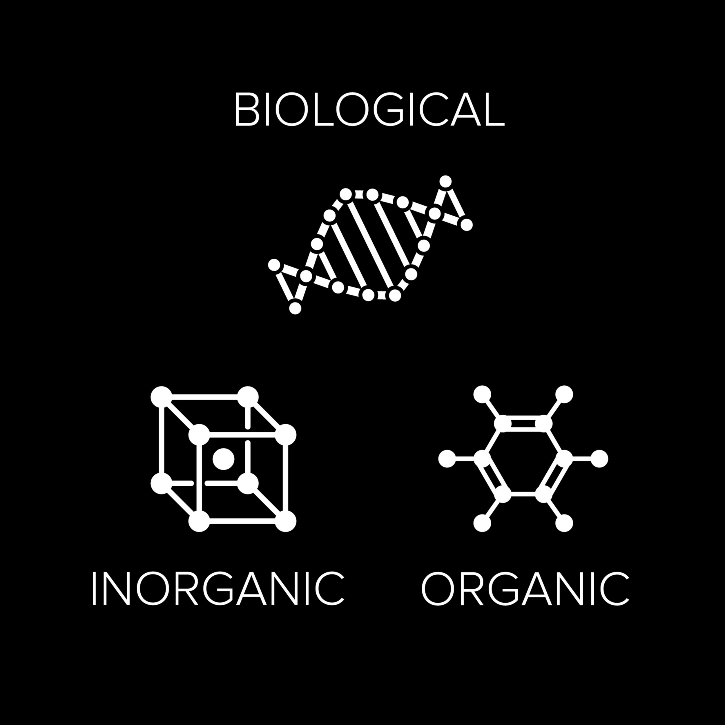
Enhanced material compatibility enables limitless patterning flexibility.
Throughput

Pattern with independent control over tens of thousands of active probes.
One instrument, limitless possibilities.
Meet E series 2.0
The first commercial beam pen lithography (BPL) tool.

Featured TERA-Fab® Applications
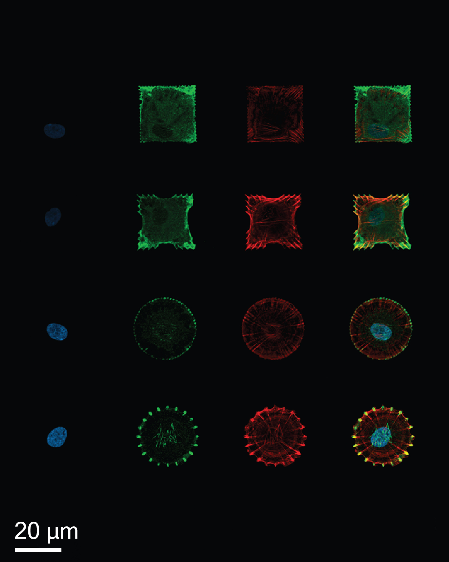
Bioengineering

Microarrays
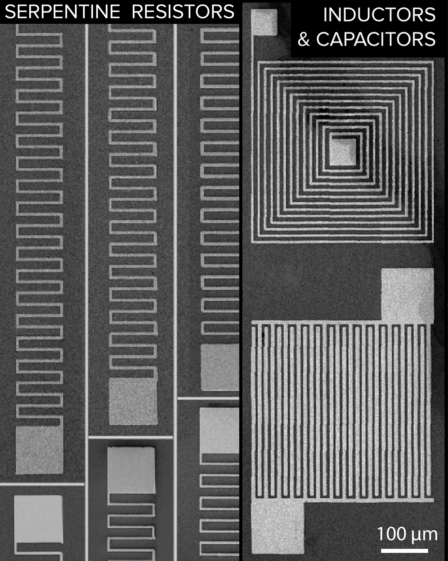
Electronics

Sensing

Microfluidics

Highly Multiplexed Photochemistry